Samsung upgrades its Texas chipmaking plant
Samsung Electronics has announced a major upgrade to its Texas plant, setting the stage to outperform its rival, Taiwan Semiconductor Manufacturing Company (TSMC), with state-of-the-art 2nm chip production in the United States by 2026. The 2nm chip technology is indeed a game-changer in the semiconductor industry. It paves the way for a new era of technological advancements, promising a future where digital devices are faster, more efficient, and more sustainable than ever before. This strategic move is part of a colossal $40 billion investment, marking a pivotal moment in the history of semiconductor manufacturing and artificial intelligence (AI) development.
Leap into future of semiconductors
The semiconductor industry has come a long way since its inception. The first integrated circuit was created in 1958, and since then, the relentless pursuit of miniaturization and performance enhancement has driven the evolution of chips. Today, we stand on the brink of a new era with the advent of 2nm technology, which promises unprecedented computational power and efficiency.
Samsung’s HBM3E chip, recently endorsed by Nvidia’s chief Jensen Huang, exemplifies the cutting-edge advancements in chip technology. The new fabrication plant in Taylor, Texas, will not only manufacture these sophisticated microprocessors but also focus on advanced chip packaging and R&D efforts.
The US Chips and Science Act plays a crucial role in this development, providing Samsung with up to $6.4 billion in direct funding. This support reflects the strategic importance of reducing reliance on foreign chip production, especially given the potential risks of natural disasters or geopolitical conflicts in East Asia.
By 2026, Samsung’s Taylor facility will commence the production of 2nm chips, a full two years ahead of TSMC’s planned production in Arizona. This aligns with the Biden administration’s goal to boost domestic advanced chip production from zero to 20 percent of the global supply by the decade’s end.
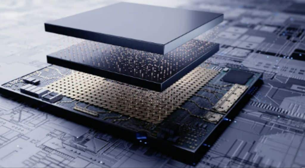
The significance of advanced packaging cannot be overstated, as it is essential for the creation of AI chips like Nvidia’s H100, used in training generative AI systems such as OpenAI’s ChatGPT6. Samsung’s investment includes a second fab for 2nm and 4nm chips and an advanced chip packaging facility capable of “2.5D packaging,” a process crucial for combining processor and memory chips in AI products. Samsung’s commitment to innovation and its strategic investment in the US semiconductor industry represent a major step forward in securing the nation’s chip supply chain and reasserting its leadership in technology. With these developments, Samsung is not only enhancing its competitive edge but also contributing to the broader goal of technological sovereignty and security.
Benefits of 2nm chip technology
The 2nm chips are set to play a crucial artificial intelligence role. They are vital for the production of advanced AI chips like Nvidia’s H100, which is used to train generative AI systems. This opens up new possibilities in AI development and applications. Despite their immense capabilities, the 2nm chips are incredibly compact. The technology enables the fitting of 50 billion transistors in a space roughly the size of a fingernail. This miniaturization does not compromise performance, making 2nm chips a technological marvel.
Imagine a world where your laptop functions at lightning speed, your cell phone battery lasts for days, and data centres have a minimal carbon footprint. This is not a distant dream but a reality that’s unfolding with the advent of 2nm chip technology. The semiconductor industry is witnessing a significant milestone with the introduction of 2nm chips. These chips are set to outperform the current 7nm node chips by a staggering 45 percent, offering enhanced performance that will revolutionize computing.
But it’s not just about speed. Energy efficiency is a critical factor in our era of hybrid cloud, AI, and the Internet of Things. The 2nm chips are expected to consume 75 percent less energy than their 7nm counterparts, making them a sustainable choice for our power-hungry digital world. One of the most exciting prospects of these advanced 2nm chips is the potential to quadruple cell phone battery life. Imagine only needing to charge your devices every four days, a convenience that will transform our digital lifestyles. In the quest for sustainability, the 2nm chips stand out with their potential to significantly reduce the carbon footprint of data centres, which currently account for one percent of global energy use. This is a significant stride towards a greener future.
The benefits of 2nm chips extend beyond personal devices and data centres. They promise to drastically speed up a laptop’s functions, from processing applications to assisting in language translation, and even speeding up internet access.